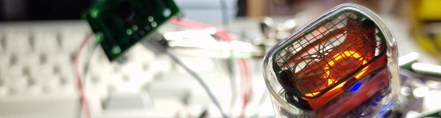
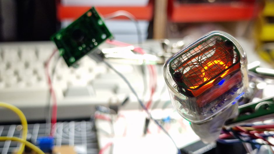
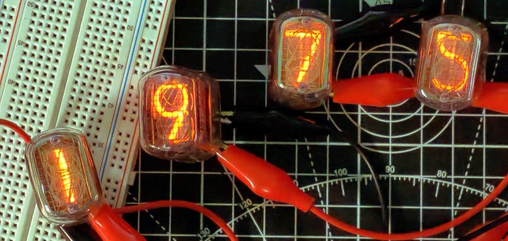
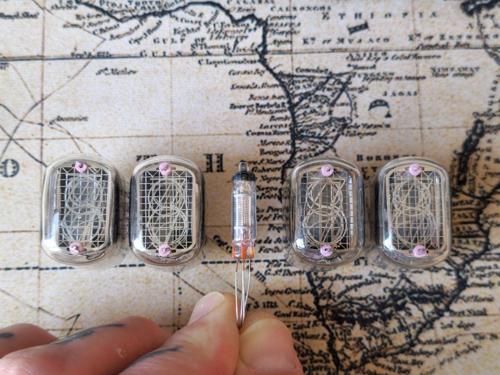
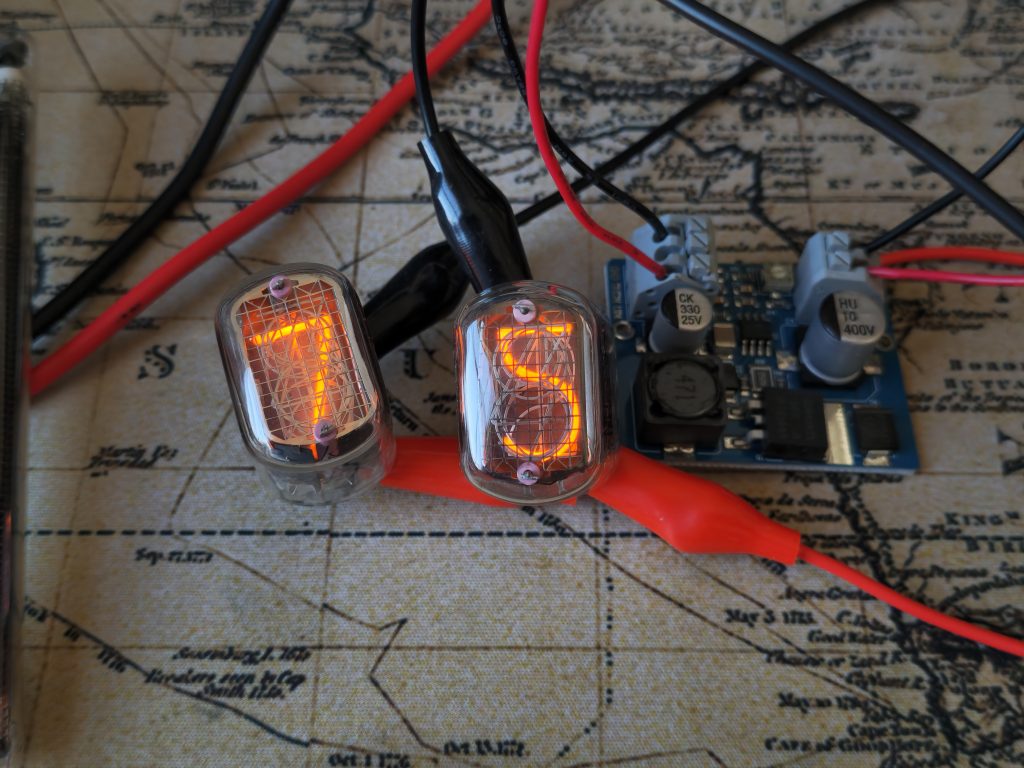
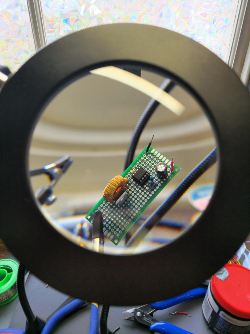
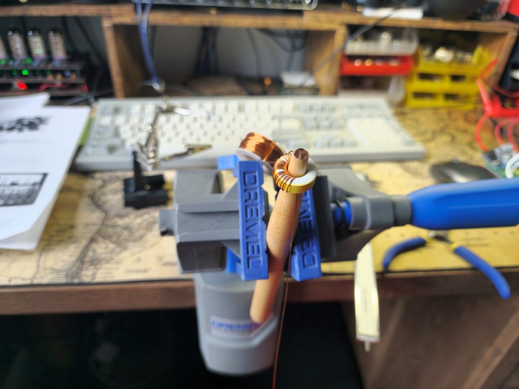
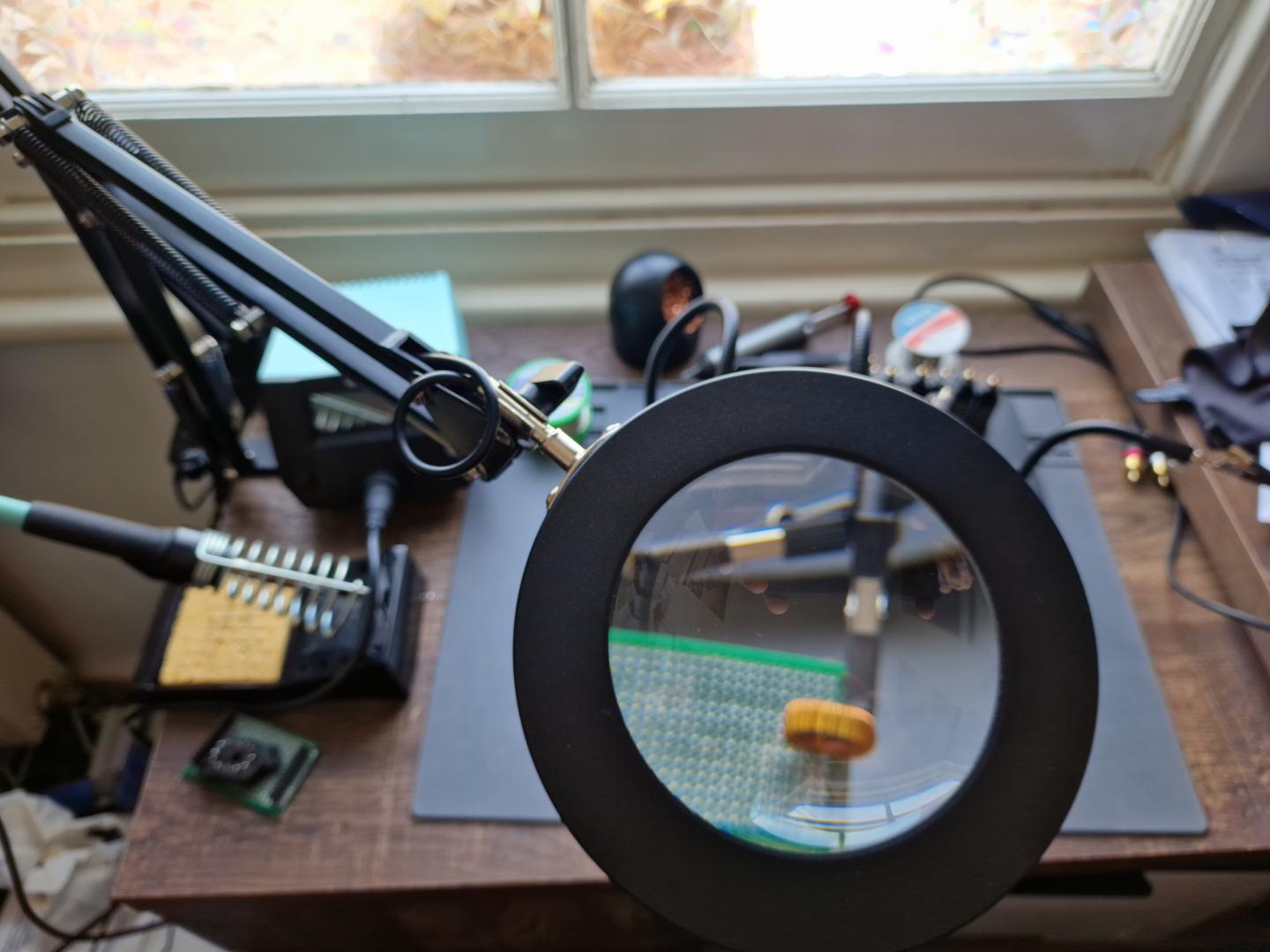
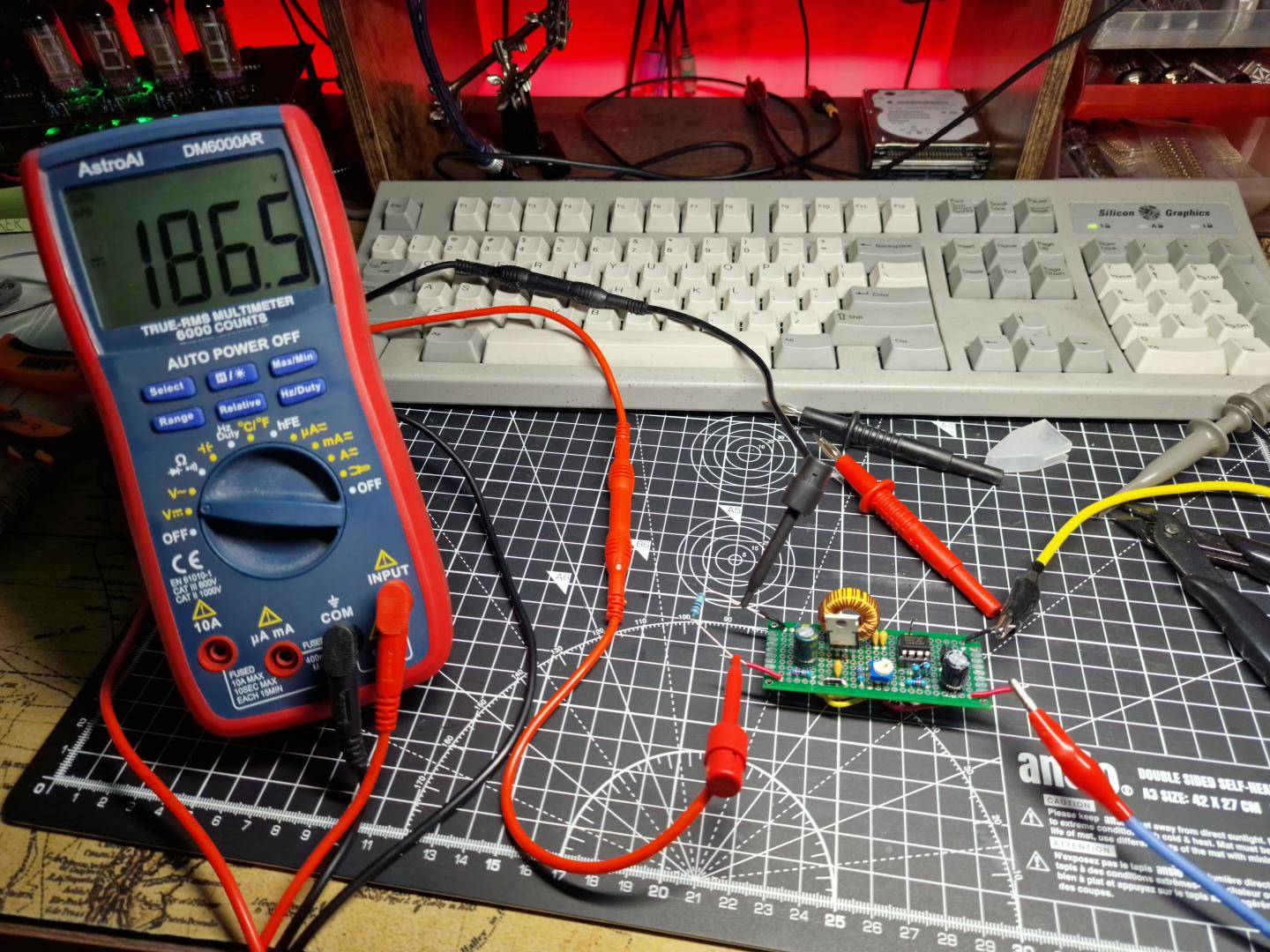
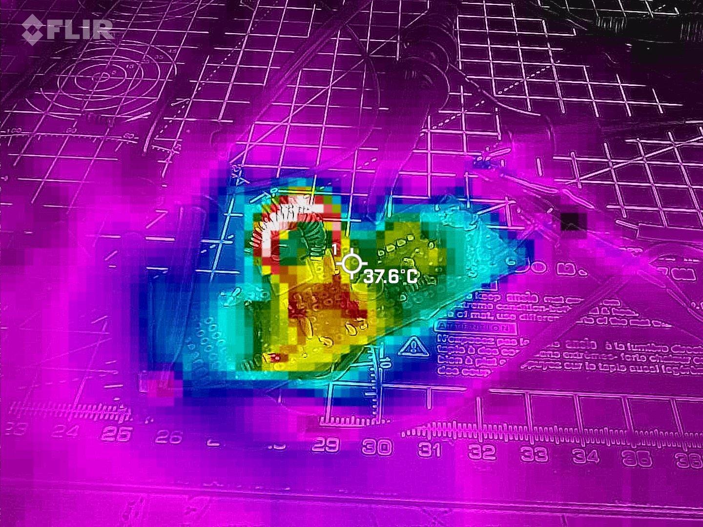
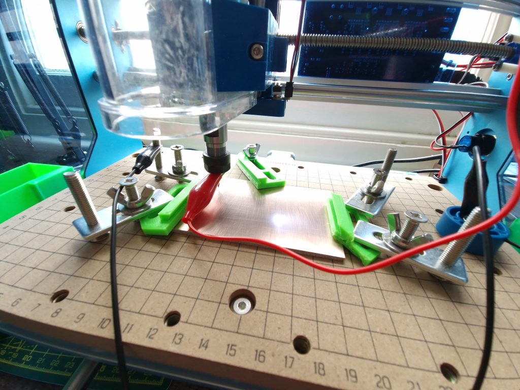
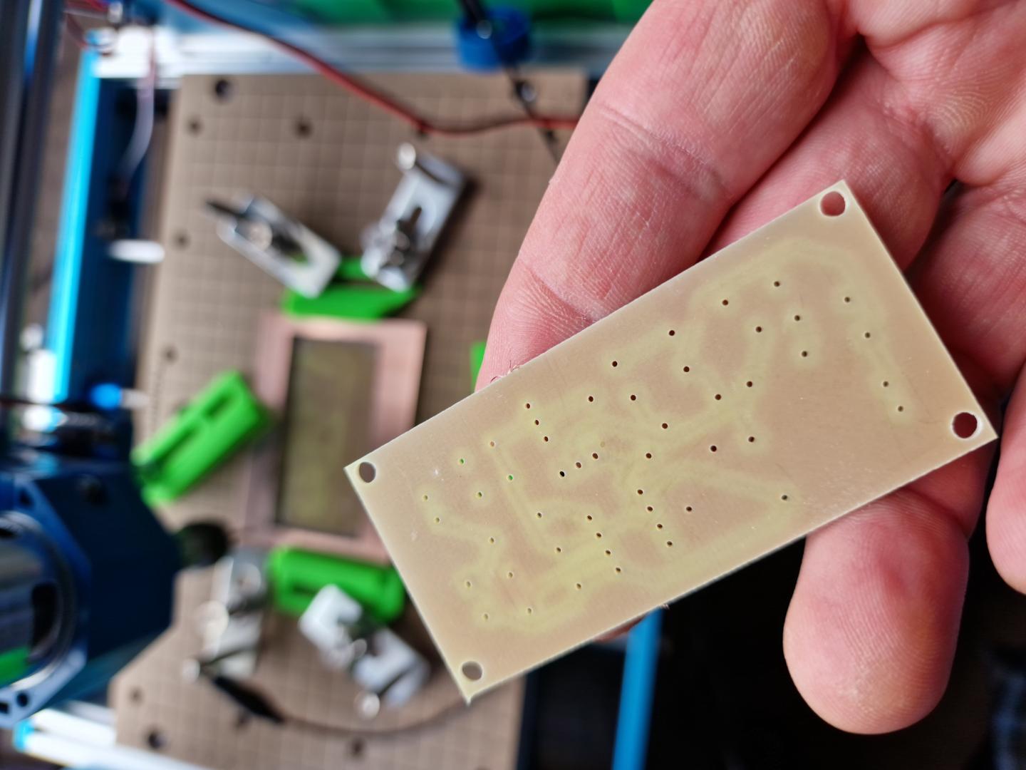
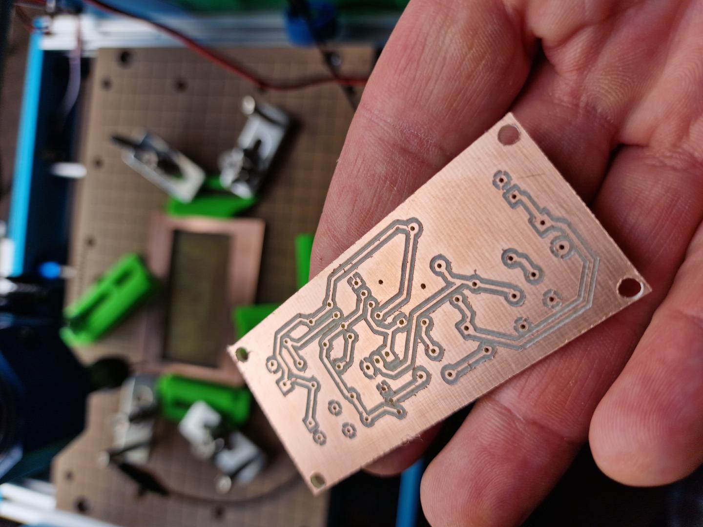
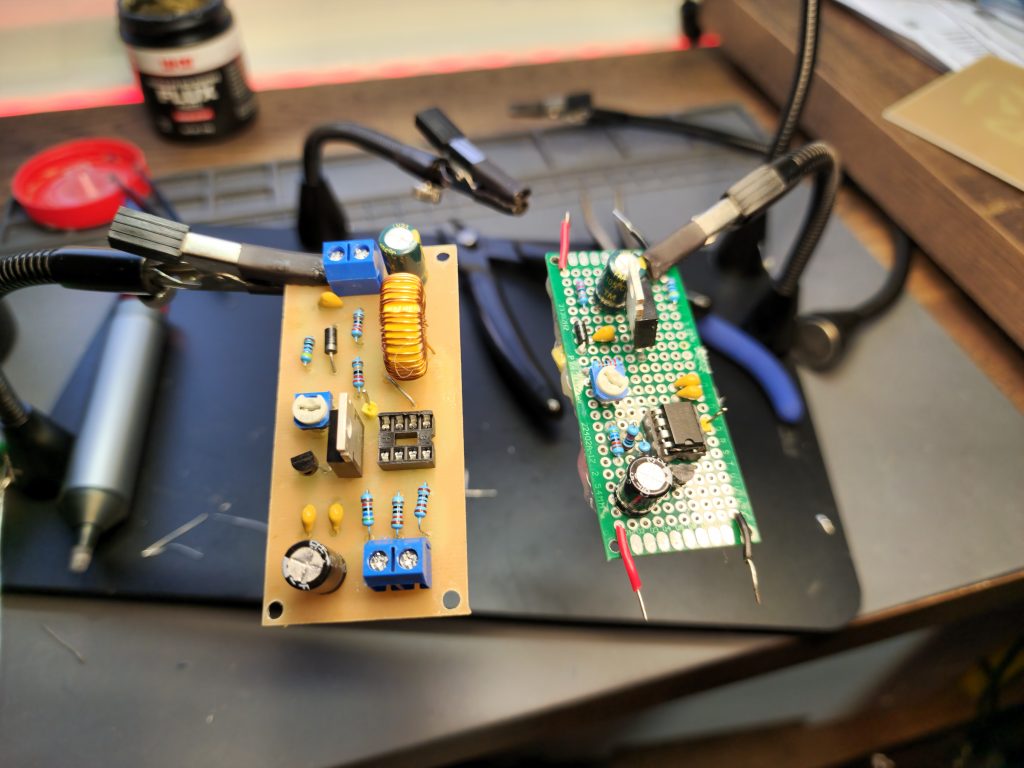
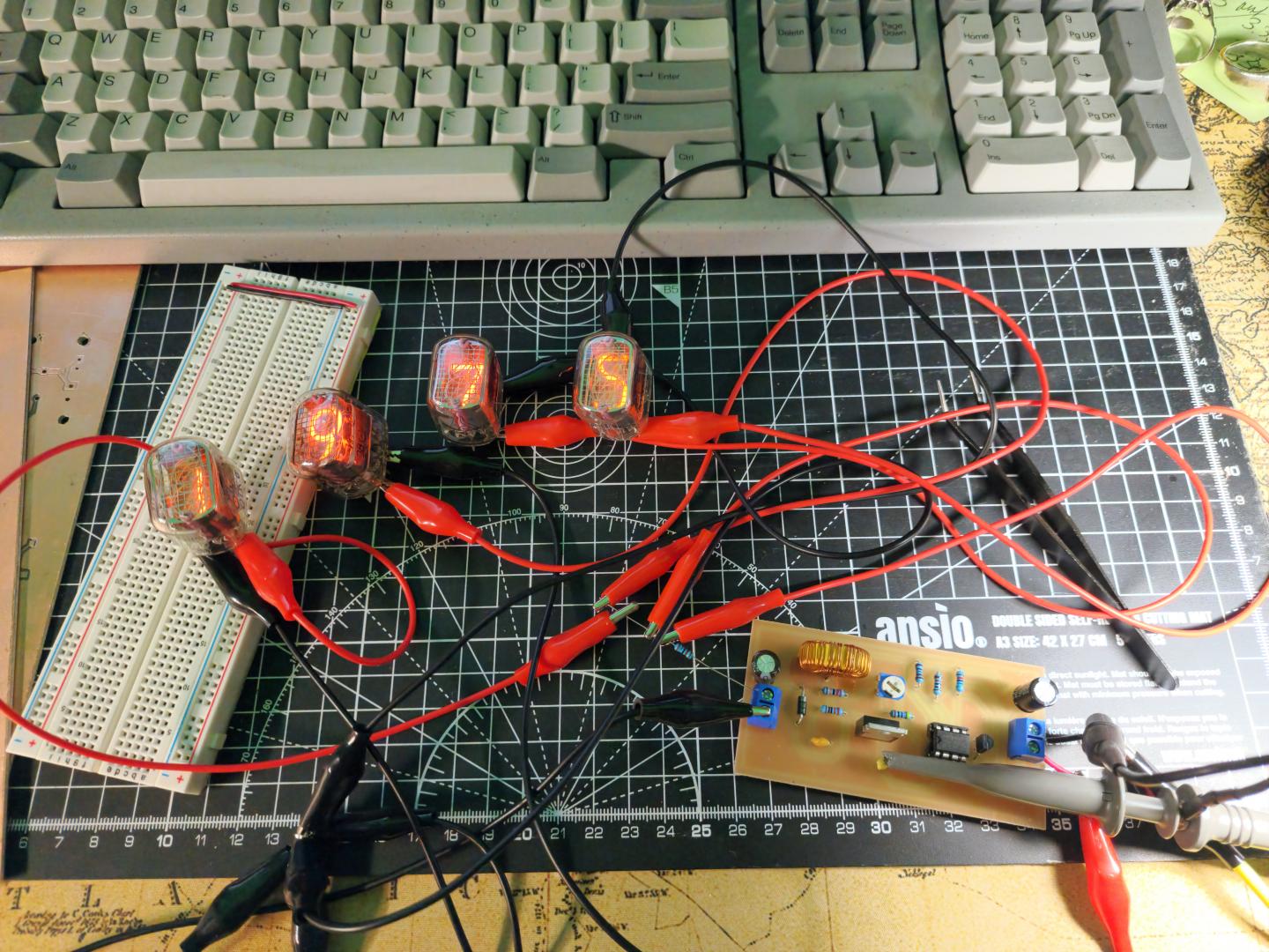
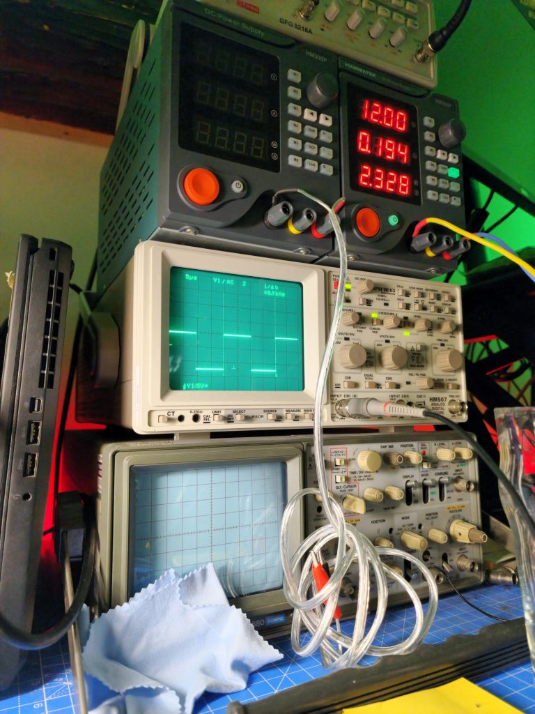
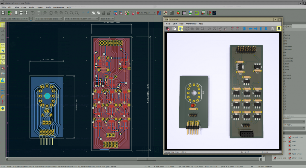
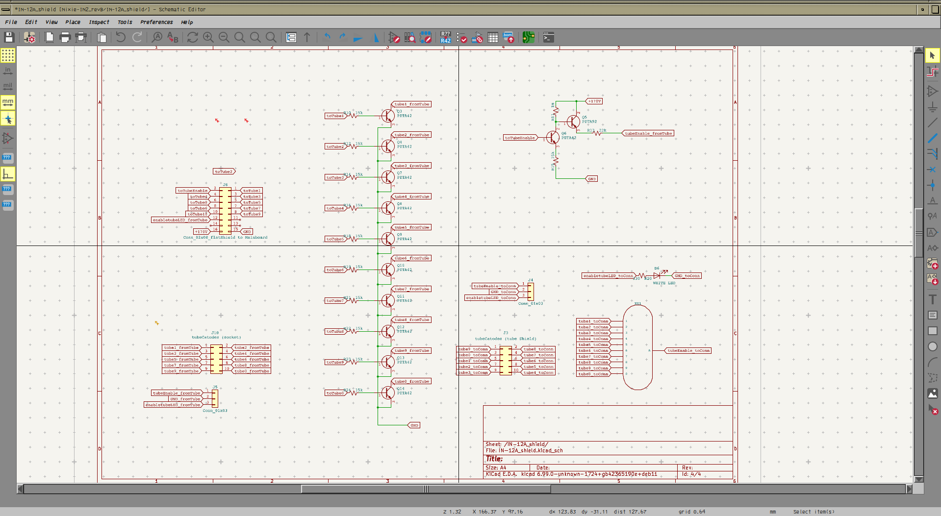
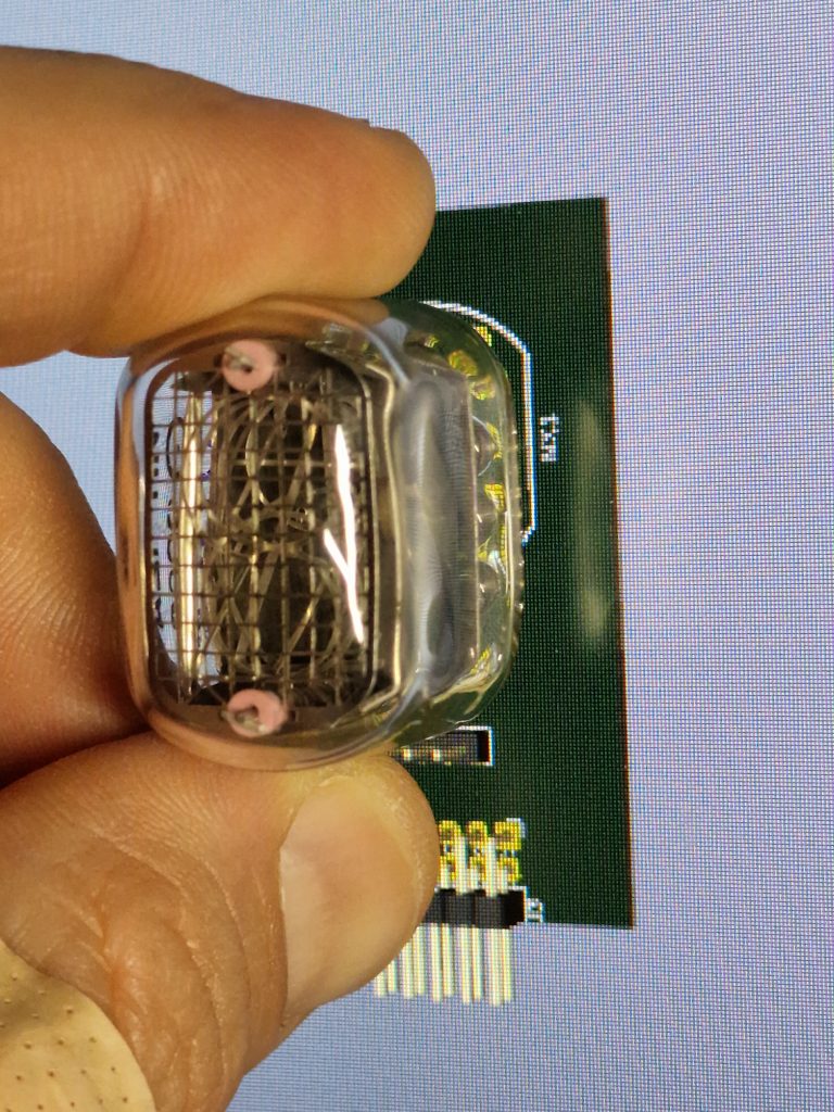
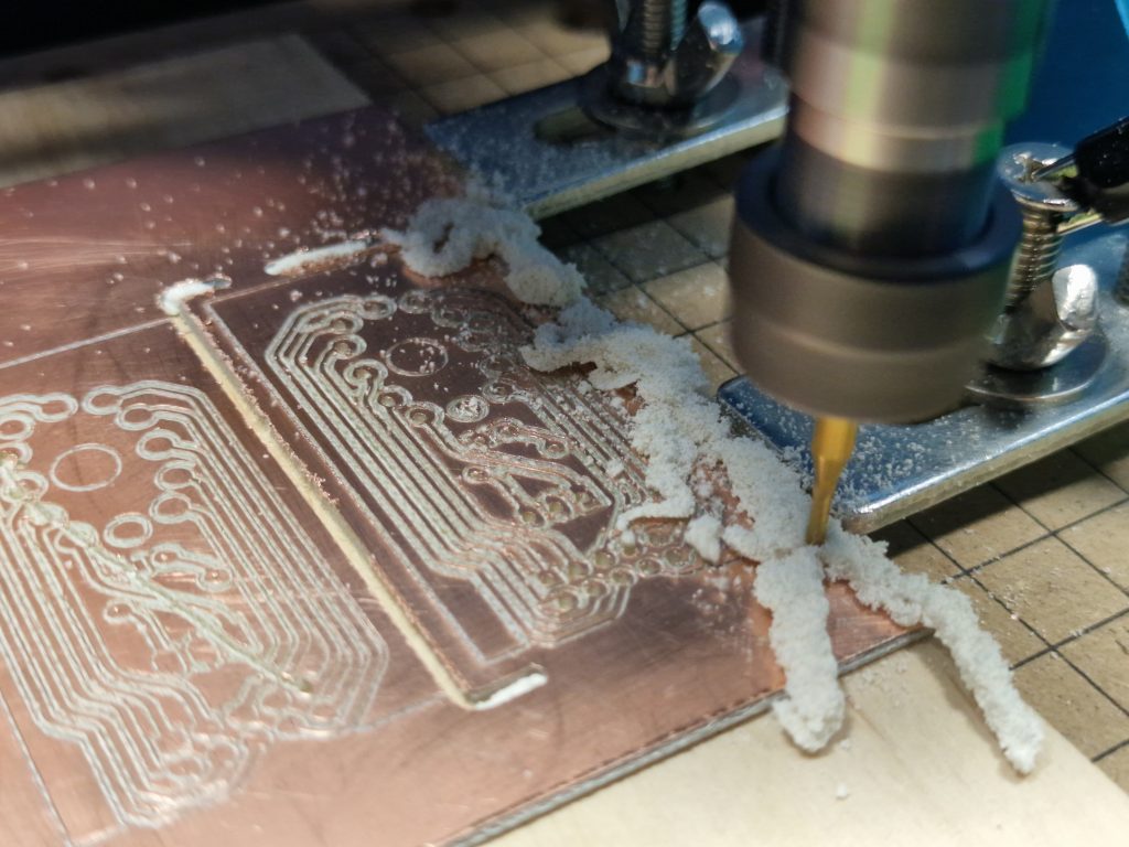
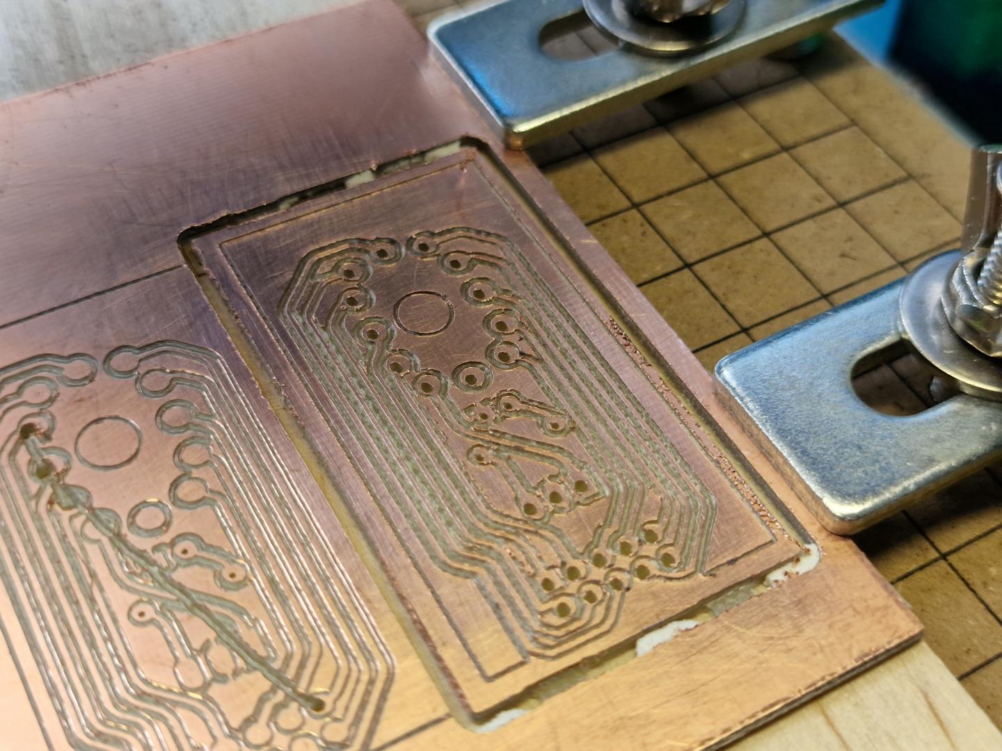
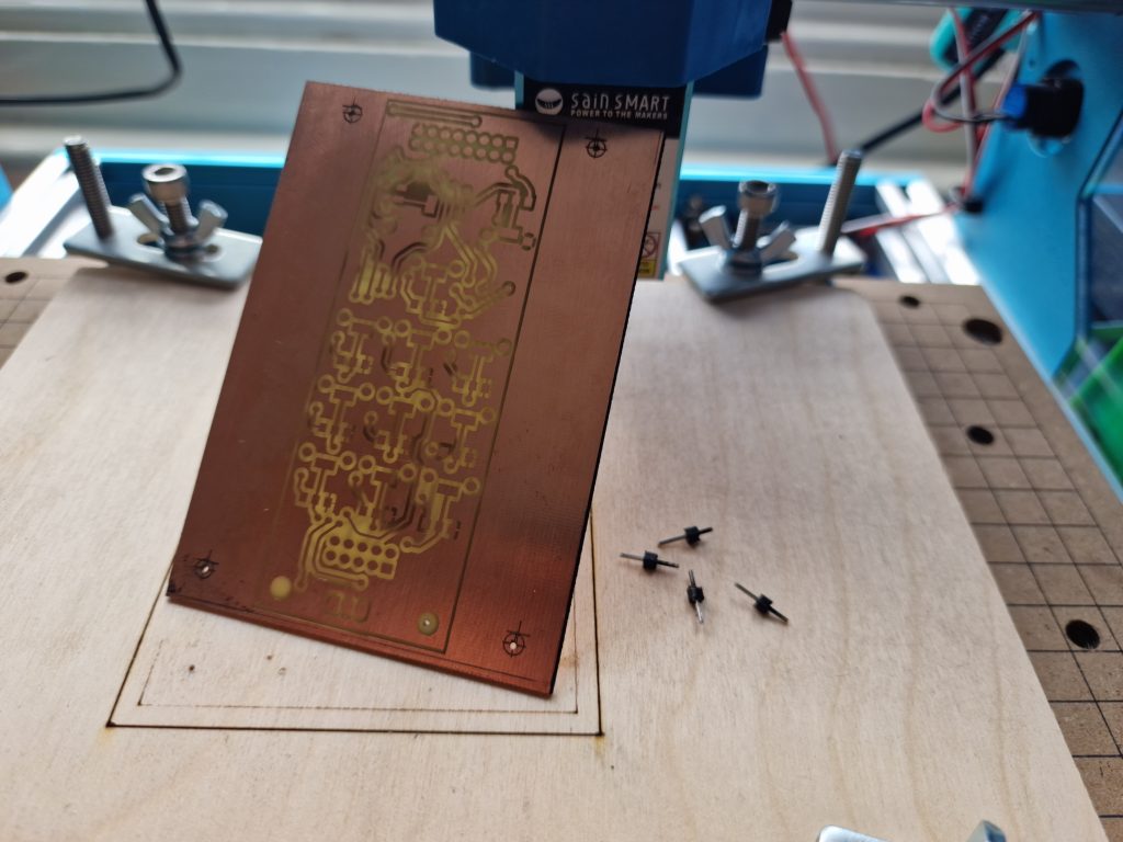
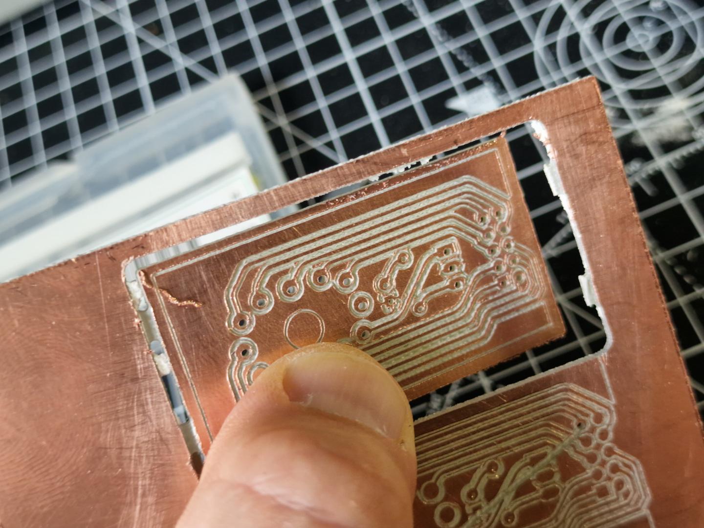
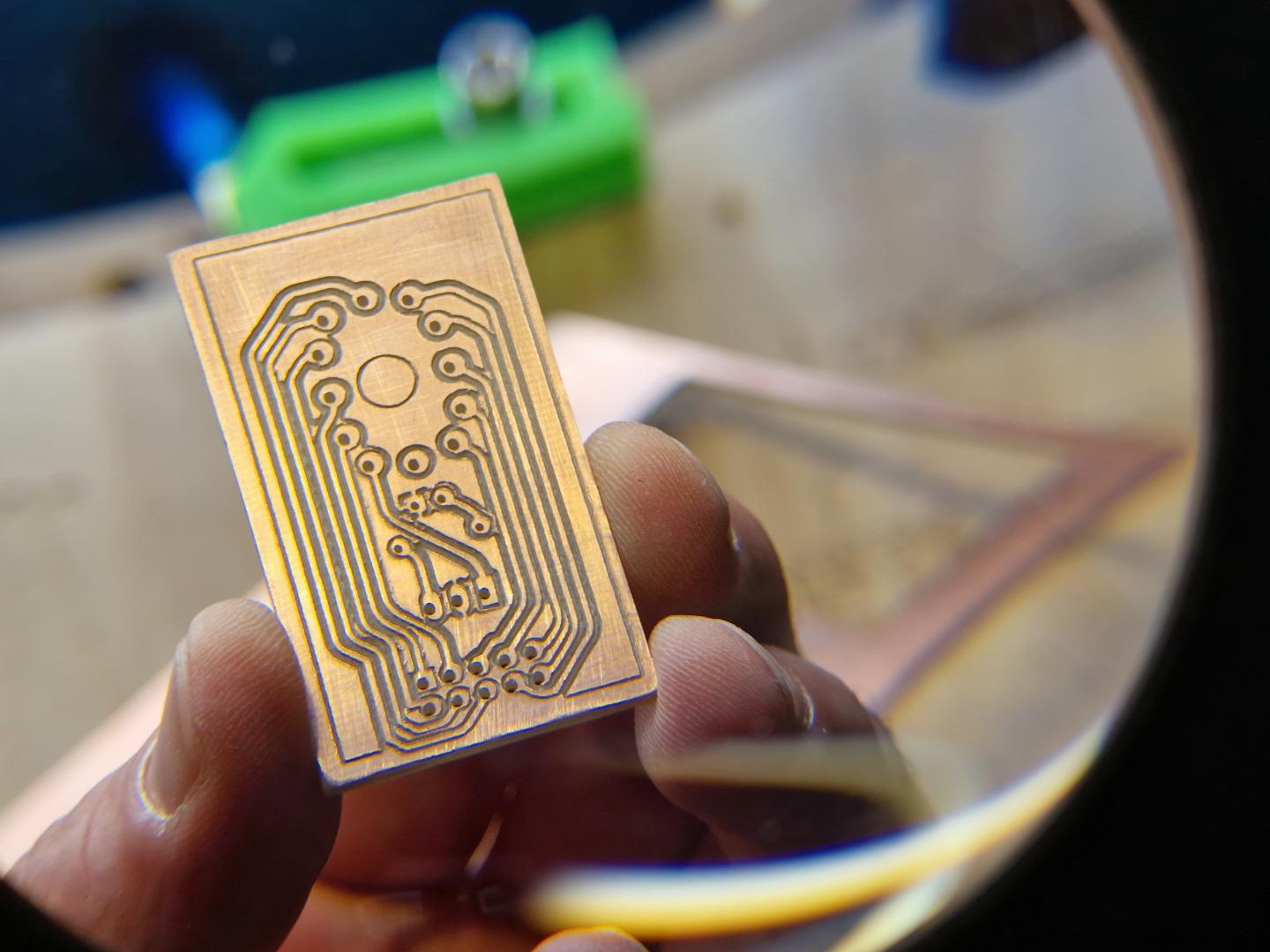
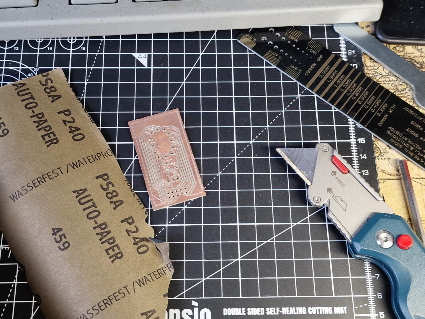
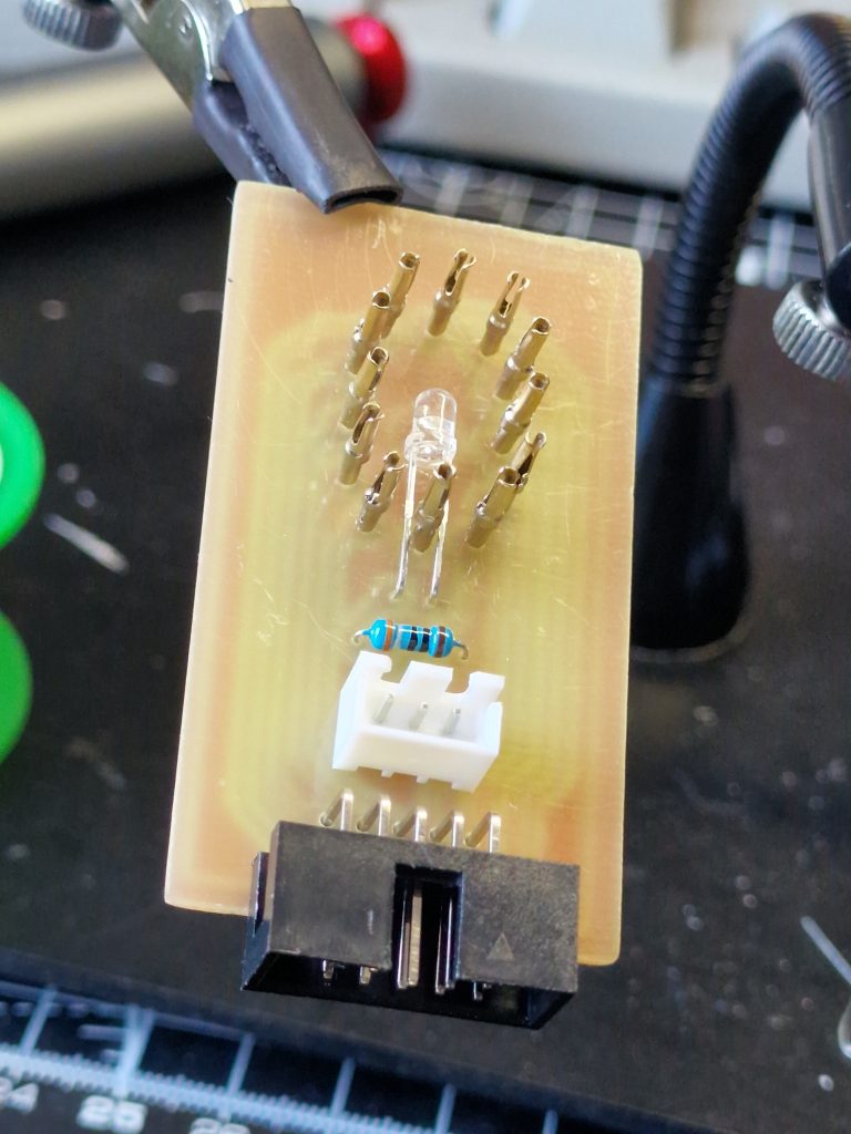
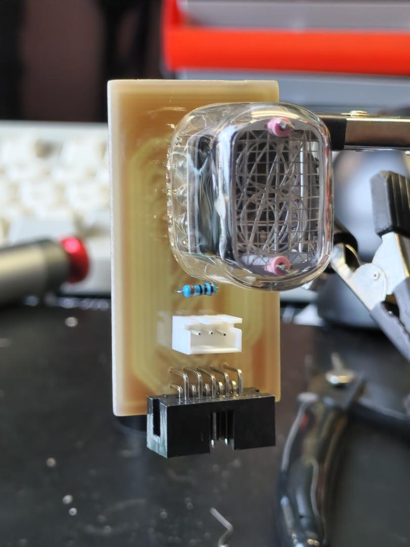
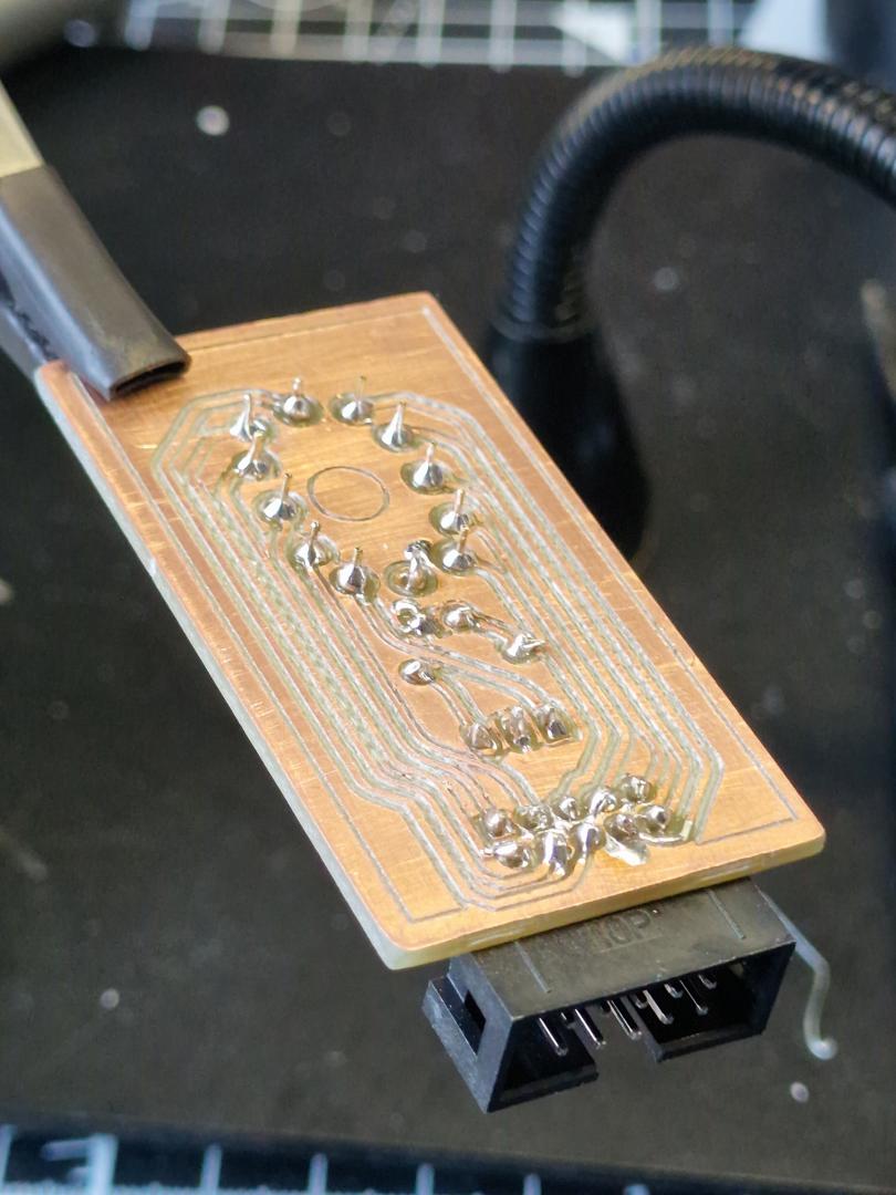
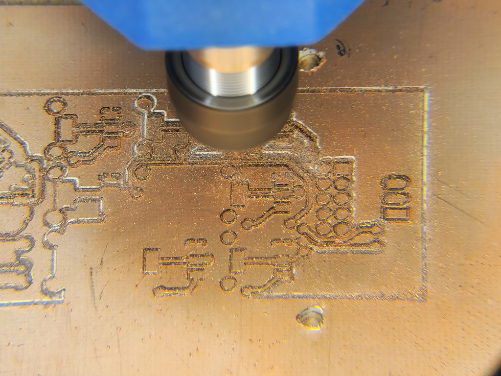
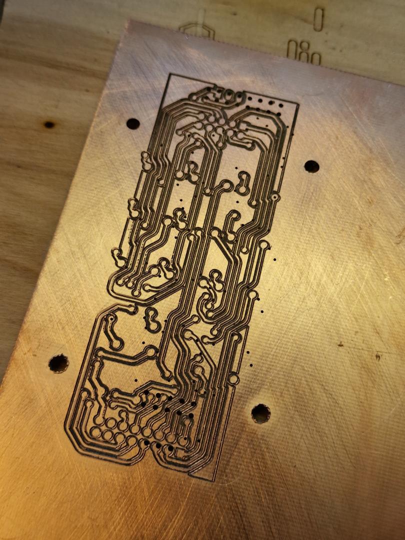
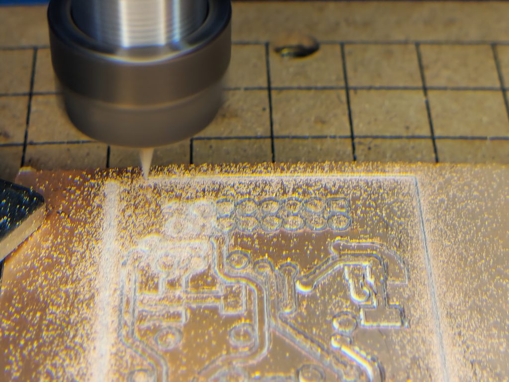
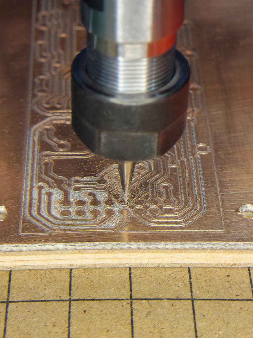
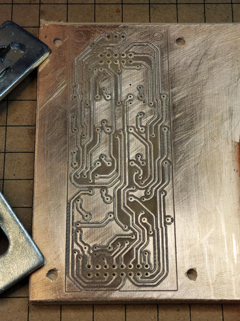
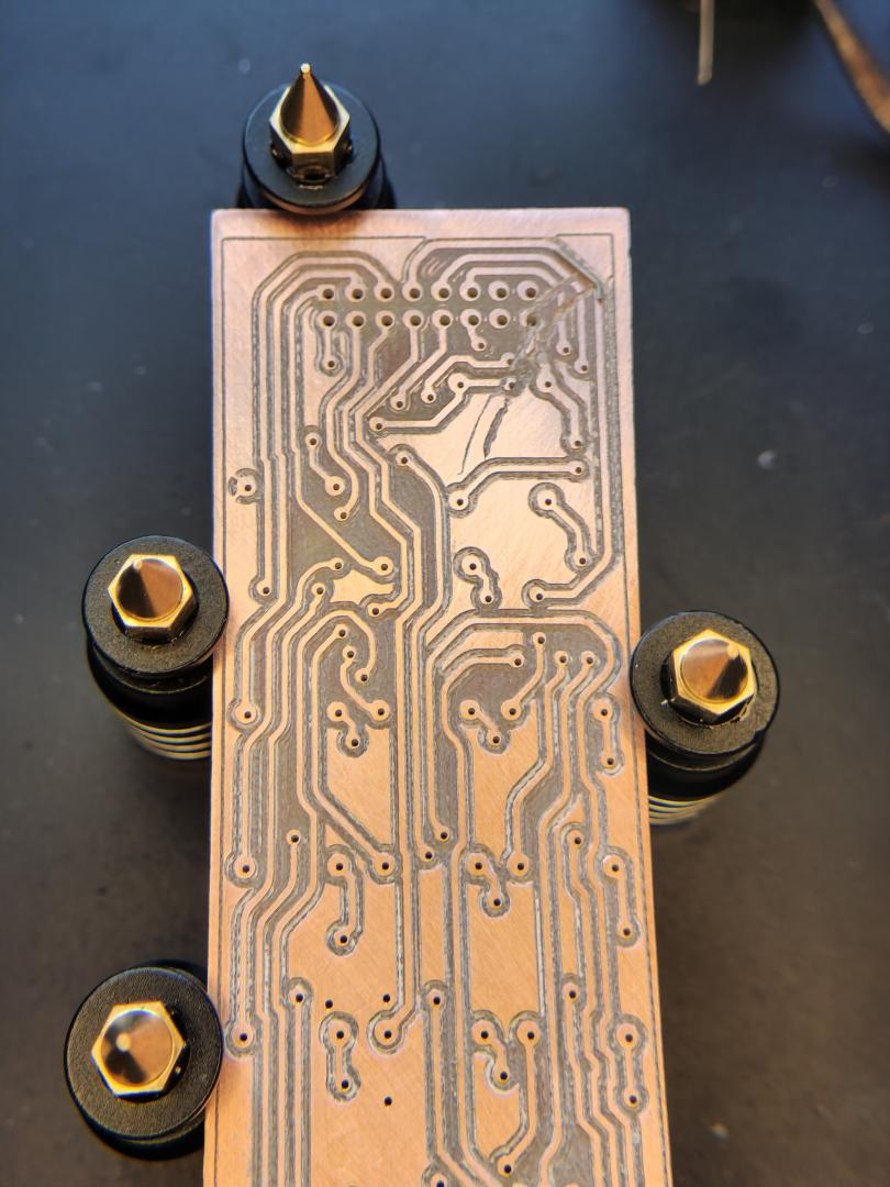
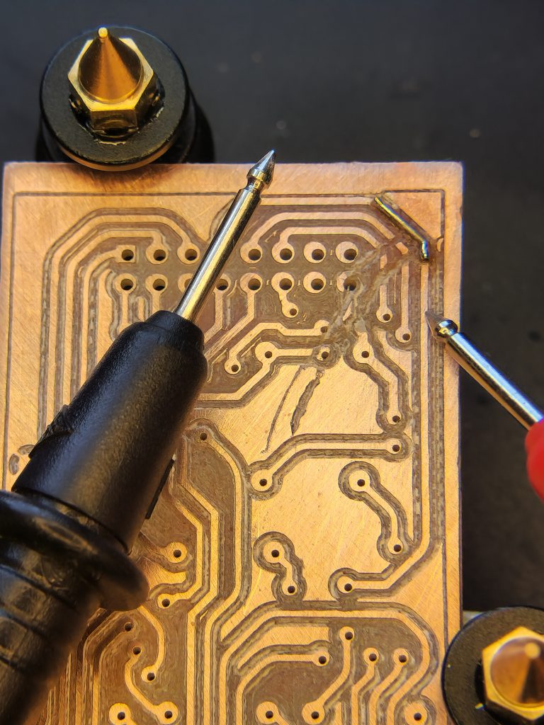
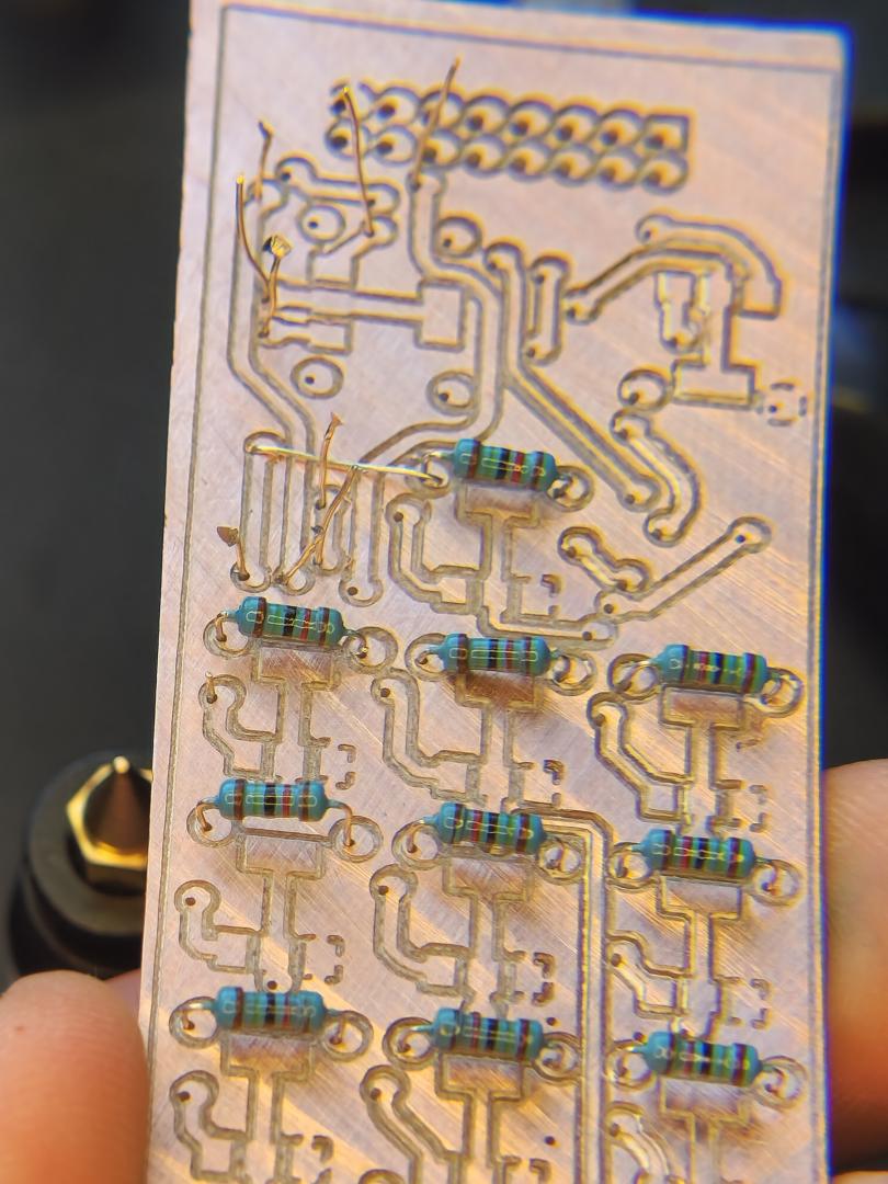
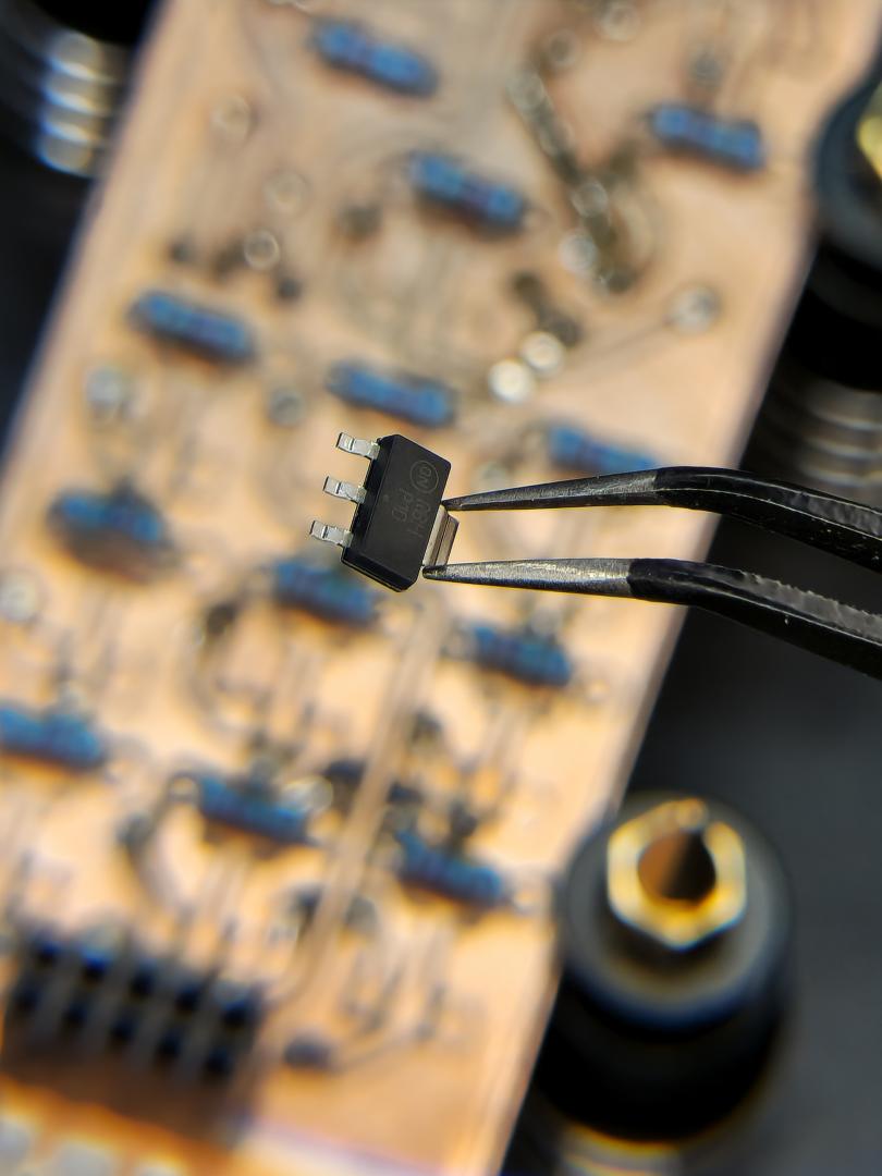
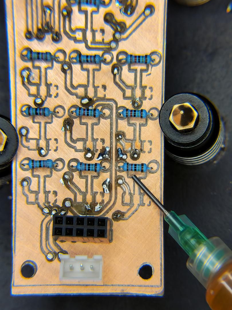
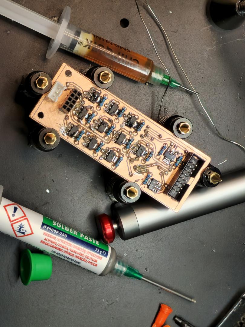
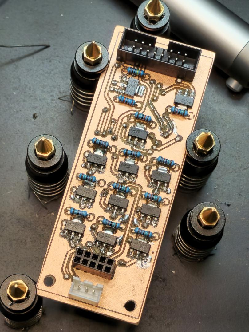
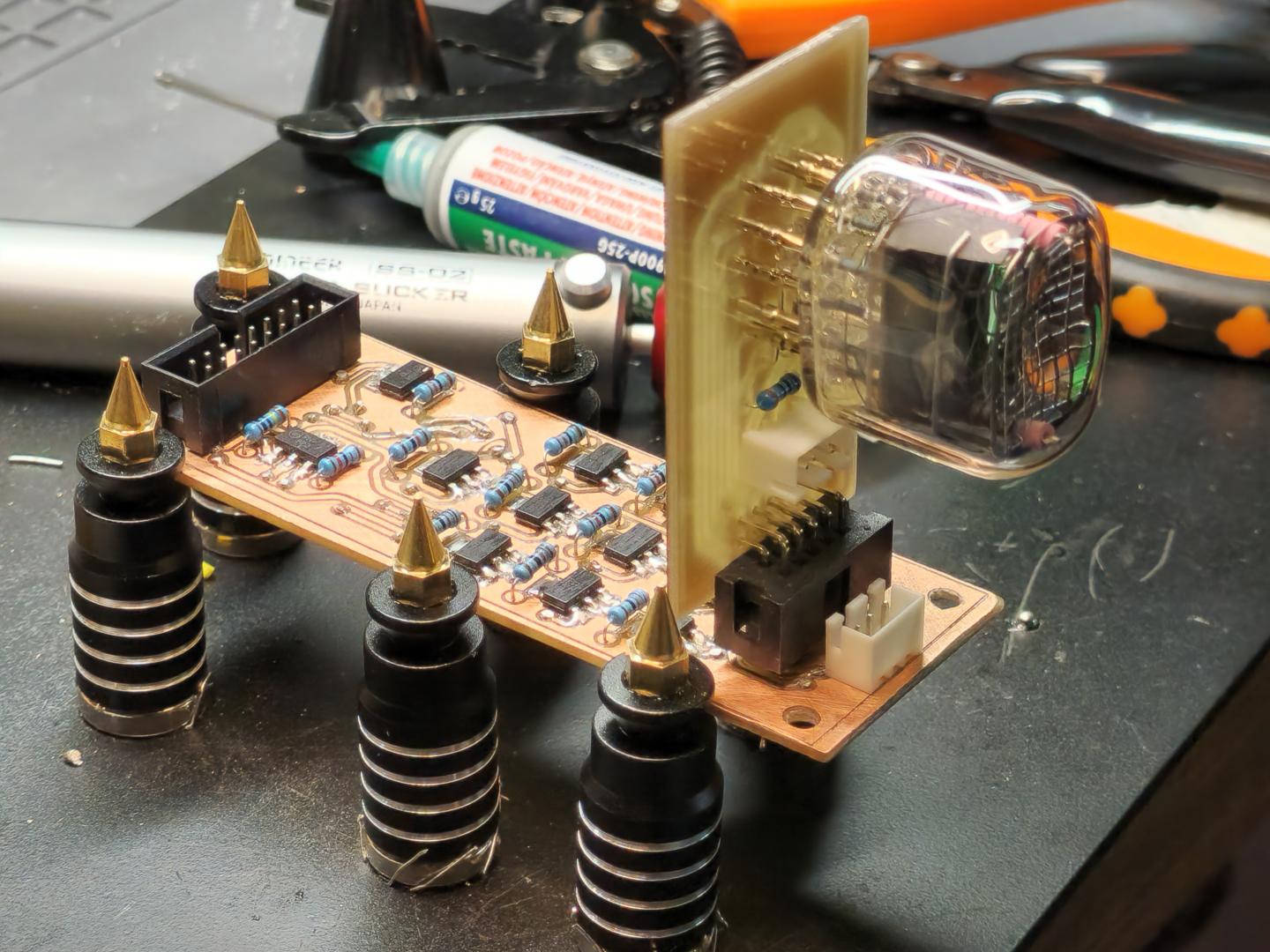
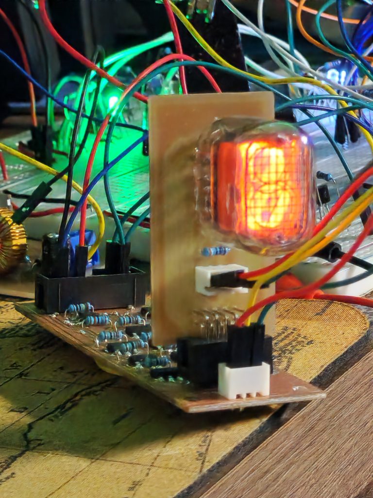
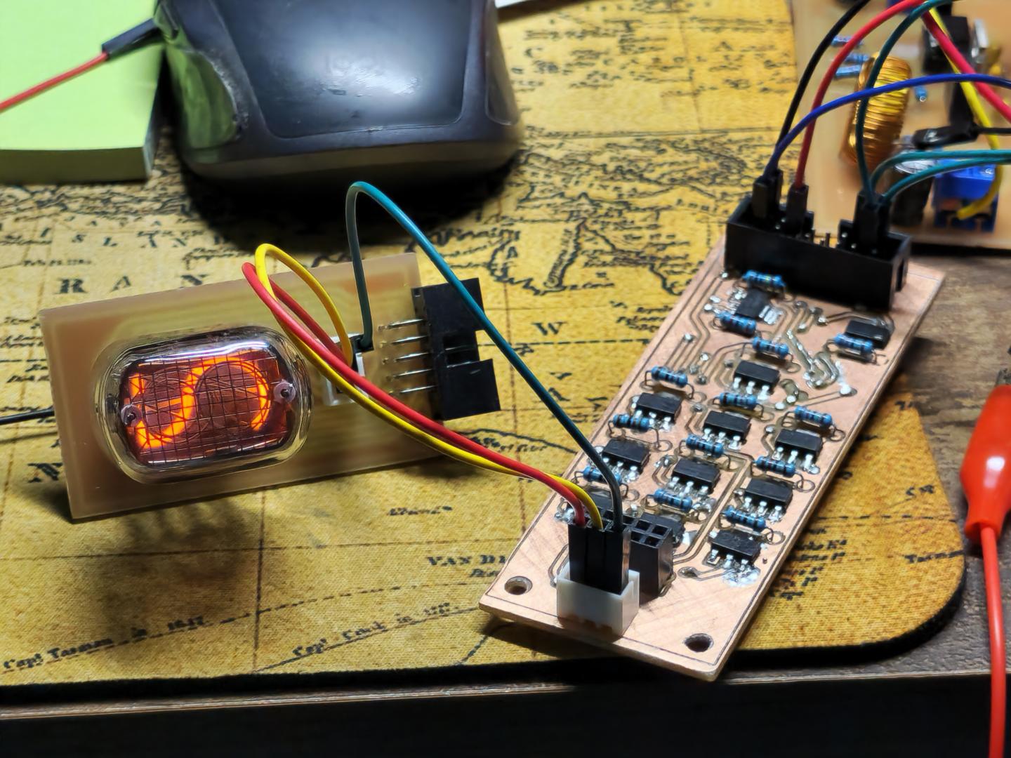
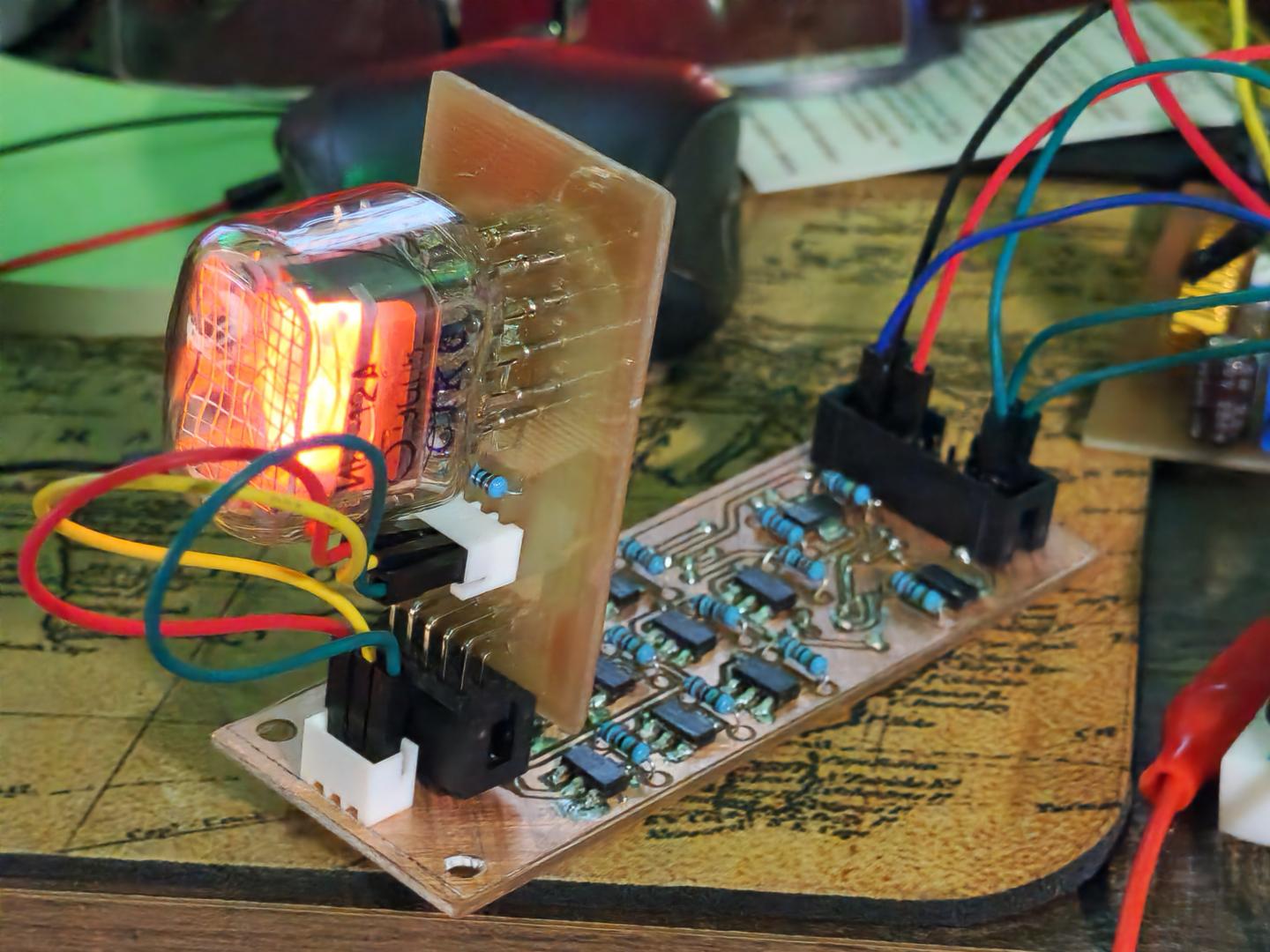
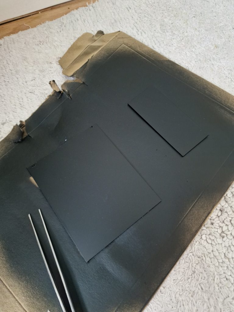
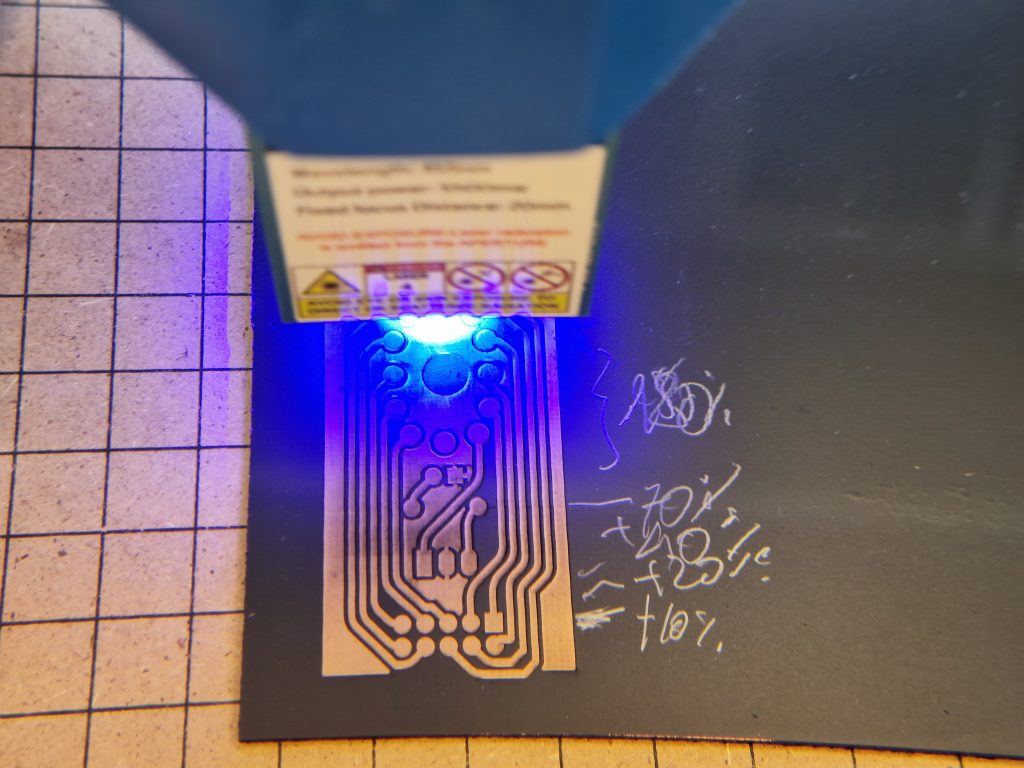
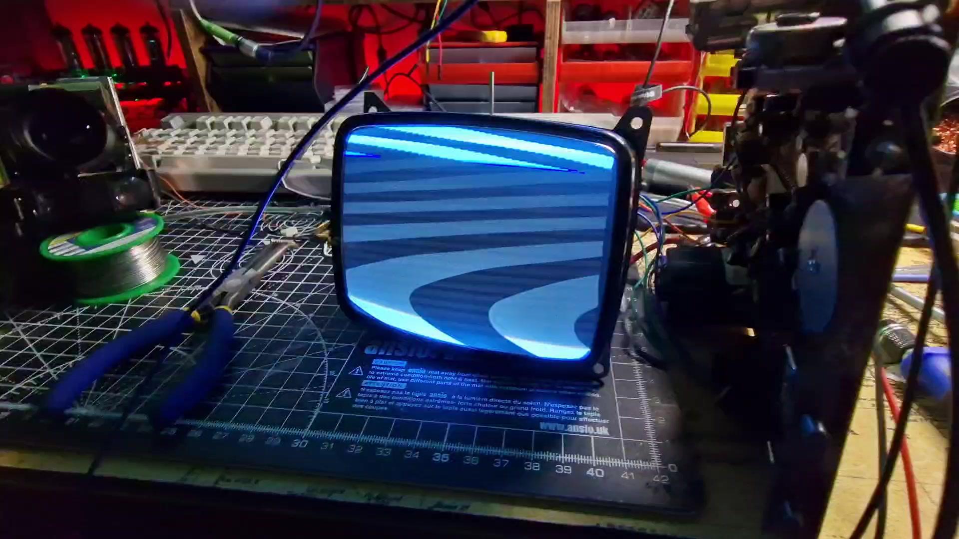
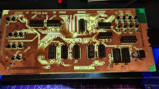
I just recently picked up again working on my first Nixies clock and here I’ll try and keep a photo diary of my progress. Stay tuned! (I’ll try and post a list of all the online resources and links I’ve used for this project) Layout for the IN-12A digits tubes and I’m still undecided between this tiny Nixie or a dot- vfd tube for the blinking seconds indicator. The clock will have vertical shields boards for the digits and flat boards for the main circuitry. To try and extend the life of the tubes in decided to use some motion detection to turn the anodes on or off. More to come. First test with a switching power supply I bought from ebay. This power supply is needed to feed the 170/180 Volts a Nixie tube needs to glow.But for this clock I wanted to build my own parts, just like for the VFD clock, and this time also including all bucks and boost converters, or switching power supply in this case. So I did some research and tried to find the simplest way to get 180V out of a 12V main supply. This is my first pcb prototype. Luckily, the Nixies tubes only source around 3.5mA, so despite the fairly high voltage involved this whole clock should run on no more than 4-5 Watts. I haven’t done the proper calculations for this yet.Learning how inductors work was the first new challenge in this project. Quite fascinating aspect of how a power supply works! After scavenging materials from old computers PSU and buying some new enamelled copper cable, and get some help for the inductor calculation, here’s my first attempt to build the 100uH inductor. Seems to work! Temperature check, passed 🙂 For my VFD clock I’ve learnt how to hetch PCB using a laser printer and Ferric Chloride, which is a really fun but “can-be” messy process at the same time. After some research I decided to grab a CNC router from amazon and try milling them instead! …. and I tell you, I didn’t expect this thing to be this loud!! (WARNING : sound is LOUD) It took several attempts (and broke countless cutting bits) to get my first Pcb properly milled, drilled and cut! For the silk screen I’m planning on laser engraving the board, at least for the single sided boards.This is what looks like a successful one!.. Except I soon realised I didn’t mirror the traces in FlatCAM and my pcb was only good as a fancy key chain! But after a few more extra hours trying to get FlatCAM and Candle to work on my Debian (to drive the CNC router) , I finally got a working milled PCB! Here’s the complete prototype. .. and a first test drive shows this is going well so far. Testing the switching power supply with the four tubes connected. My old VFD clock was adjusted with buttons, for this one I wanted to use rotary encoders and potentiometers. This is my first setup using flip-flops to decode whether I’m spinning clockwise or counter clockwise. Using a DA1010 logic analyser I can check whether the de-bouncing circuit is working well. First test drive of the tubes using a signal generator and the motion sensor. All good so far! Time to start designing the individual PCBs.From the schematic to the PCB design. I think I’ll get the tubes for the digits assembled into multiple boards connected via either cables or pin headers… This step will take a while! It’s like playing a puzzle game. A fairly long one, too.Pcb design ain’t an easy job, specially when you’re limited to 2 layers, thick traces, and very little experience! But all seems connected, according to the DRC rules check! Weekend plans is to trace these boards on the CNC router, possibly laser engrave the silk screen, definitely to solder all the components and check whether this modular IN-12a shields will work well for the final project! Yup, I just can’t wait for the board to be ready 😂👍 After a few weeks trying to understand why Lightburn was failing every single job I’ve decided to give up and use Lightburn for the gcode generation only, then send the gcode straight from Candle. After some tweaking I got a nicely etched double sided board 🙂 next step is to burn a solder mask layer (yet have to decide what material to use for that one) and then align the FlatCAM drill job to Lightburn, or rather to the current work space coordinates. Today I’ve managed to find some decent settings for the milling of the Tube shield. Took quite a bit to find the right bit to use, the depth and the milling feed (speed).. For this first board I’ve skipped the copper clean stage as I had too many failures trying, but the traces have good continuity and the board doesn’t seem to have any shorts. A bit of sanding and this is ready to get the components soldered!Whilst the CNC router is milling the driving board here’s the tube shield assembled. Not my finest board for sure, but I can’t wait to see it in action! Etching PCB was a process that took me quite a few failures before I could get consistent positive results, and a system that worked nicely and reliably. With PCB milling I’m back to square zero on the learning board again, and failure will be part of the learning process of a completely new approach to me. These photos show a fail on a double side board, which took me several passes to try and get the traces properly scraped off the board, and then realise I flipped the PCB clad copper board on the wrong axis when milling the back side. A weekend of failure for sure, but failure is where you grow and learn. Tonight has been a long one. I think I’ve managed to find some decent settings for a good board milling, even tried a layer of copper removal. However, after these past two weeks of late nights and weekends trying to get this done, I think I’ll switch back to etching and use this CNC router for the the drilling, cutting and the laser engraving stages only. After fixing a few problems, both from a mistake made during milling and from some wrong board design, I’ve managed to solder all the components, including the vias. For this project I’ve also used some SMD transistors, first time for me to try and deal with surface mounted components and let me tell you, its both fascinating and scary to deal with such tiny things. These are SOT-223, so possibly the biggest version of them. Solder flux and paste from a siringhe and some good magnifier lens, and lots of patience. Job done! Unfortunately there’s some issue either with the board or the PCB routing, all the cathodes get lit when connected to the driver board. This means its time to call it a night, finally get some food and leave this to rest for a few days until I’ll try and find the problem. I’m definitely going to put this on the side for a few days. Will come back to this soon! My weekend task, laser engraving the traces and etch the board. Let’s try with this new approach! I think I quite like this approach! The paint has been beautifully burnt by the laser (1500mm/min, power 100% on a 5.5W blue laser) and next step is etching to see how the copper will handle it! Very promising so far!
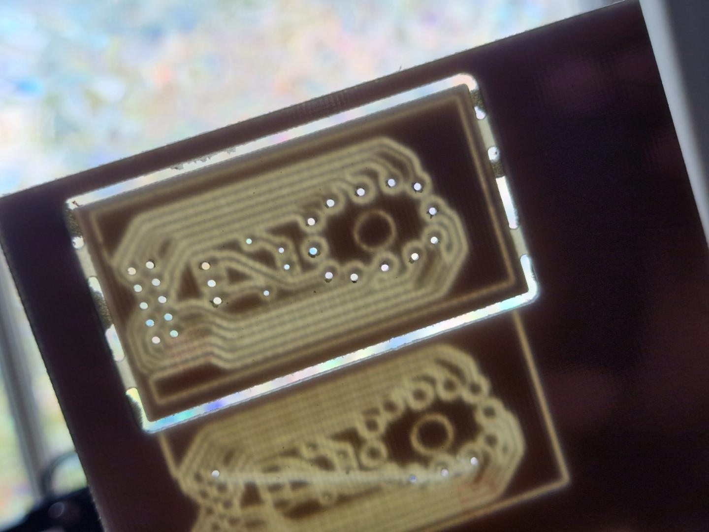
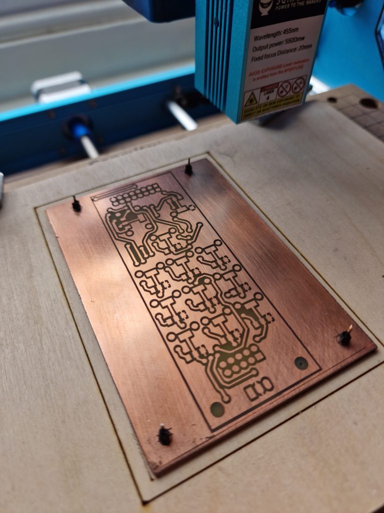
Using a four corners pinned alignment for the two sides worked pretty well. This is the etched board on both sides. Next step swapping the laser for the spinner, then drill and cut. But before that I want to try is laser cutting a solder paste mask.